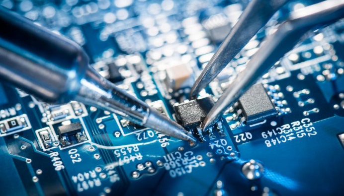
Crystal oscillators are often referred to as the "heart" of digital circuits because all operations rely on clock signals. The oscillator directly controls the entire system—if it fails, the system halts. Thus, a high-quality crystal oscillator is a prerequisite for digital circuit functionality.
Modern high-frequency crystal oscillators emit strong harmonic interference, which can propagate through input/output traces and radiate spatially. Poor layout design may lead to severe noise radiation issues that are difficult to mitigate later. Therefore, careful PCB placement of the oscillator and clock signal traces is critical.

Key PCB Design Guidelines for Crystal Oscillators:
1. Decoupling Capacitors: Place them as close as possible to the oscillator's power pins. Arrange capacitors in descending order of capacitance along the power flow path, with the smallest capacitor nearest to the power pin.
2. Grounding the Case: The oscillator's metal casing must be grounded to reduce its radiation and shield against external interference.
3. Keep-Out Area: Avoid routing traces beneath the oscillator. Ensure a solid ground plane and maintain a 300mil (7.62mm) clearance around the oscillator to prevent interference with other traces, components, or layers.
4. Clock Trace Design: Keep clock signal traces short and wide. Balance trace length with distance from heat sources.
5. Edge Avoidance: Never place the oscillator near the PCB edge, especially in card-type designs.